In the rapidly evolving field of ceramic additive manufacturing, multi-material ceramic 3D printing is revolutionizing the production of ceramic electronic devices. This advanced technique enables the creation of high-temperature ceramic electronics and conductive ceramic structures that withstand extreme environments while delivering superior performance. At Shenzhen AdventureTech Co., Ltd. (ADT), a leader in ceramic 3D printing solutions since 2015, we empower researchers and manufacturers to harness these innovations through our precision DLP ceramic 3D printers, high-performance materials, and one-stop services.
This comprehensive guide explores the groundbreaking process of multi-material ceramic 3D printing for durable electronic devices, drawing from cutting-edge research published in Materials Today. By integrating intrinsic material-based catalytic metallization with multi-material vat photopolymerization (MM-VPP), manufacturers can produce robust, damage-free 3D ceramic electronics. ADT’s expertise and equipment make this technology accessible and scalable for your applications.
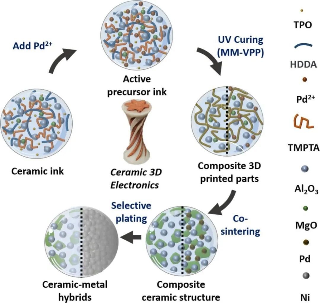
Figure 1: Overview of the multi-material ceramic 3D printing process for ceramic-metal hybrids. This schematic illustrates how Pd²⁺-doped active precursor inks combine with standard ceramic inks during MM-VPP printing, followed by co-sintering and selective electroless plating to form precise conductive ceramic structures.
Why Multi-Material Ceramic 3D Printing Matters for Ceramic Electronic Devices
Traditional ceramic manufacturing struggles with conductivity and complex geometries. Ceramics like Al₂O₃ excel in high-temperature resistance, chemical stability, and mechanical strength—ideal for high-temperature ceramic electronics—but they are insulators by nature.
Multi-material ceramic additive manufacturing solves this by enabling spatial control of active and inert ceramic regions in a single print. Active zones incorporate Pd²⁺ ions that reduce to Pd nanoparticles during sintering, acting as catalytic “nano-anchors” for selective metal deposition (Ni, Cu, or Ag). The result? Fully integrated conductive ceramic structures with embedded 3D conductive networks that maintain structural integrity at temperatures exceeding 600°C.
ADT’s self-developed DLP ceramic 3D printers and optimized slurries are engineered to support these multi-material workflows. With over 10,000 slurry and sintering tests and 40+ exclusive patents, ADT delivers the precision and reliability needed to turn research into production-ready ceramic electronic devices.
The Step-by-Step Process: Ceramic Additive Manufacturing Meets Selective Metallization
The process begins with two Al₂O₃-based slurries: an inert ceramic slurry and an active slurry containing Pd²⁺. Using MM-VPP 3D printing, active and inert regions are precisely encoded within the same part. After printing, multi-stage debinding and high-temperature co-sintering densify the ceramic while converting Pd²⁺ to catalytic Pd(0) nano-anchors. Selective electroless plating then deposits conductive metals exclusively in active zones.
This damage-free approach ensures perfect pattern fidelity—even in deep cavities and internal structures inaccessible by traditional methods.
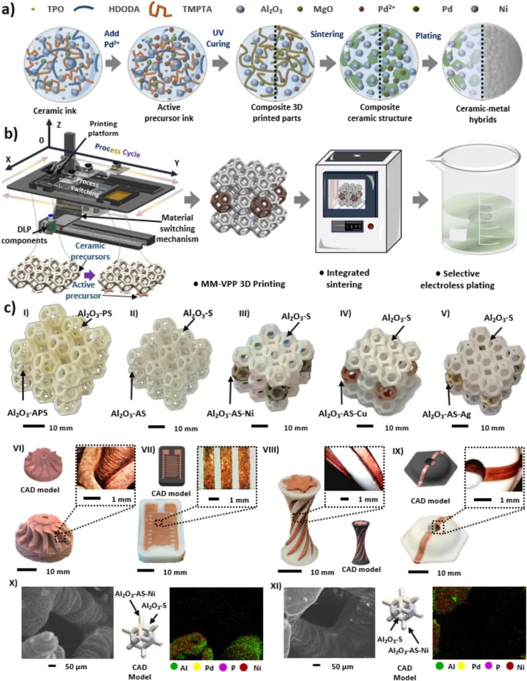
Figure 2: MM-VPP printing system and real-world examples of multi-material ceramic structures. See lattice structures, spiral conductors, and micro-lattices fabricated via ADT-compatible DLP technology, demonstrating Ni, Cu, and Ag metallization in active regions only.
ADT’s DLP ceramic 3D printers feature automated material switching and support the exact workflow shown above. Whether you need research-grade prototypes or scalable production, our equipment and materials ensure consistent results in ceramic additive manufacturing.
Material Characterization and Interface Excellence
Advanced analytics confirm the process’s reliability:
- XRD and XPS verify α-Al₂O₃ phases and Pd(0) formation only in active zones.
- SEM and EDS mapping show uniform Pd distribution at interfaces, enabling strong adhesion (4B rating per ASTM D3359, peel strength 2.6 ± 0.3 N·cm⁻¹).
- Surface roughness decreases dramatically post-sintering, yielding dense, high-precision parts.
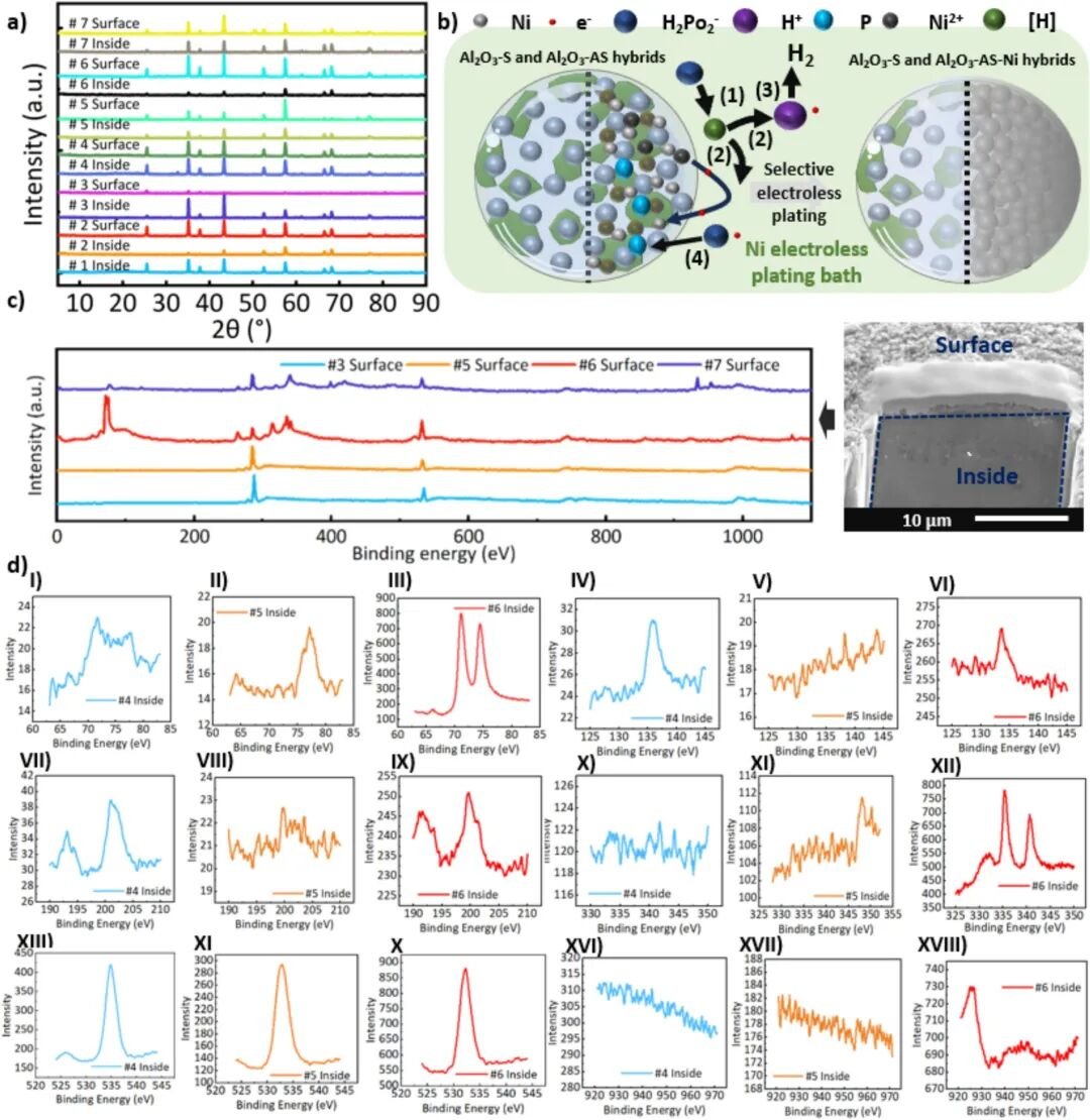
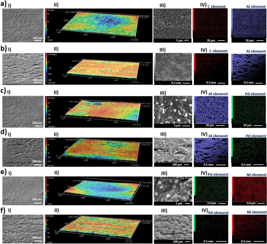
Figure 4: Surface morphology, roughness mapping, and elemental distribution in active vs. inert ceramic regions.
These characterizations highlight why conductive ceramic structures produced this way outperform conventional methods—perfect for ADT customers building reliable high-temperature ceramic electronics.
Robust Metal-Ceramic Interfaces for Extreme Environments
Cross-sectional analysis reveals a stable intermediate layer where Pd and Ni migrate strategically, creating exceptional bonding without compromising the ceramic matrix.
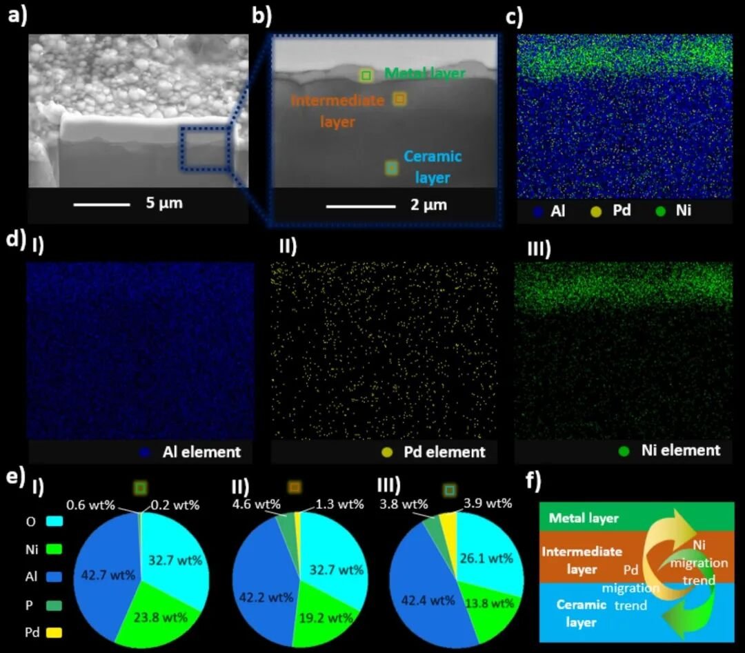
Figure 5: Cross-sectional SEM, elemental mapping, and quantitative composition of the metal-ceramic interface. This robust anchoring ensures durability under thermal cycling, damp heat, and ozone exposure—key for long-life ceramic electronic devices.
Proven Performance: High-Temperature Antennas and Low-Temperature LED Modules
Real-world testing validates the technology:
- High-temperature ceramic antennas maintain stable signal reception at 600°C, far surpassing commercial and resin-based alternatives that fail at 200–300°C.
- Ceramic LED modules deliver linear current response and uniform heat dissipation at –10°C, eliminating mismatches seen in polymer electronics.
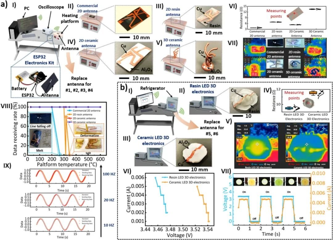
Figure 6: Extreme-environment performance testing of 3D ceramic antennas and LED electronics. Infrared thermography and waveform data confirm superior thermal uniformity and electrical stability.
Why Partner with ADT for Your Ceramic Additive Manufacturing Needs?
Since 2015, Shenzhen AdventureTech Co., Ltd. (ADT) has been at the forefront of multi-material ceramic 3D printing and ceramic additive manufacturing. Our postdoctoral R&D team from Tsinghua University, USTC, and beyond has helped over 200 universities and research centers build complete ceramic 3D printing systems.
We offer:
- Precision DLP and DIW ceramic 3D printers optimized for multi-material workflows
- High-performance Al₂O₃ slurries compatible with active/inert designs
- One-stop ceramic 3D printing services for complex conductive ceramic structures
- Expert consultation for high-temperature ceramic electronics applications
Beyond Materials, Beyond Limits. ADT is leading the future of ceramic 3D printing.
Ready to build durable electronic devices with multi-material ceramic 3D printing? Contact ADT today: adventuretech@adt-ceramic3dp.com
Visit https://adt-ceramic3dp.com to explore our full range of ceramic 3D printing solutions and book a consultation.
More articles
Multi-Material Ceramic 3D Printing for Durable Electronic Devices
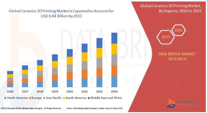
Ceramic 3D Printing Market Forecast 2026–2033: Opportunities, Growth, and Key Applications
Advanced Insights into Late-Stage Sintering: Multi-Stage Grain Growth in Ceramic Materials
Gyroid-Structured SiOC Composites via DLP 3D Printing for Broadband Microwave Absorption
Request A quote