
Industry new knowledge
Tsinghua University Li BoProfessor Team in《Advanced Materials Technologies》publish Topological Flexible 3D Microwave Perfect Absorber,The method of combining traditional absorbing materials with metamaterials to achieve perfect absorption and enhanced microwave absorption, and the performance test and theoretical analysis of the prepared microwave absorber.

Original link: https://doi.org/10.1002/admt.202302148
Adventure Technology official website: http://www.adventuretech.cn/
If it cannot be opened, please copy the URL to the browser.
research content
Absorbing materials according to the working mechanism and manufacturing process can be dividedTraditional materials and metamaterials. Traditional Material PackageincludingCarbon-based, ferrite-based and polymer-based materialsThey each have advantages and disadvantages, such as the existence of traditional materials.Limited absorptive capacity and narrow bandwidthand other issues. Metamaterials haveFlexible designThe absorption performance can be improved by adjusting the structural parameters, but the processing of high-frequency metamaterials is usuallyDifficult, time-consumingAnd the cost is high.
This study explores an innovative approach to achieve by combining traditional wave absorbing materials with metamaterials.Study on Perfect Absorption and Enhancement of Microwave Absorption. Specifically, the study integratesAbsorbing Basement Membrane (BM) and 3D Wood Stack (WP) Photonic Crystals. Both are used.Polydimethylsiloxane (PDMS) as a matrix material, combined with carbonyl iron powder (CIP) as an absorber to form a flexible composite material.
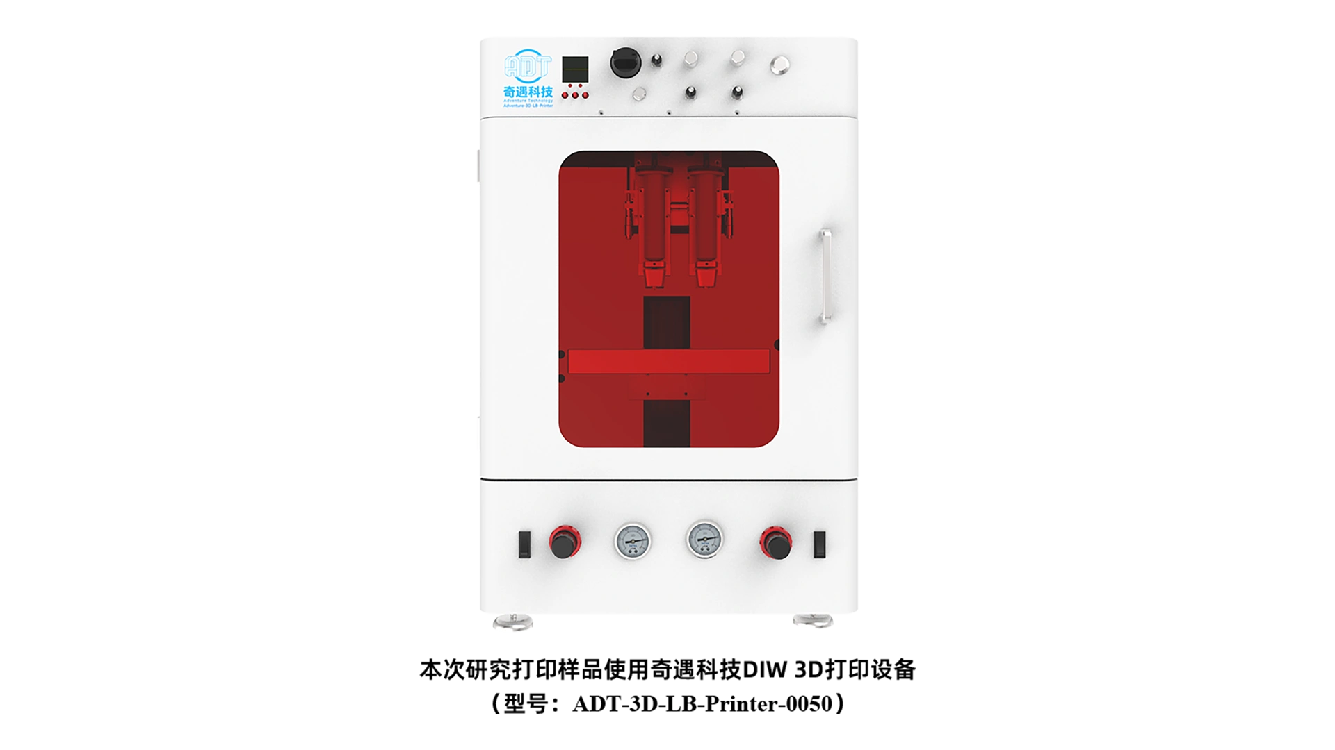
UseDirect Ink Writing (DIW)(Model ADT-3D-LB-Printer-0050) EquipmentThree-dimensional photonic crystals with single or coupled concentration absorbers were fabricated. The experimental results show that the integrated absorber10 dB bandwidth up to 10 GHz, and inWide range of angles of incidence from 0 ° to 50 °, the maximum absorptive capacity exceeds100 dB. by regulating the concentration of the absorbent in the BM,The frequency of the absorption peak can be flexibly adjusted between 6 and 16 GHz. The specific steps are as follows:
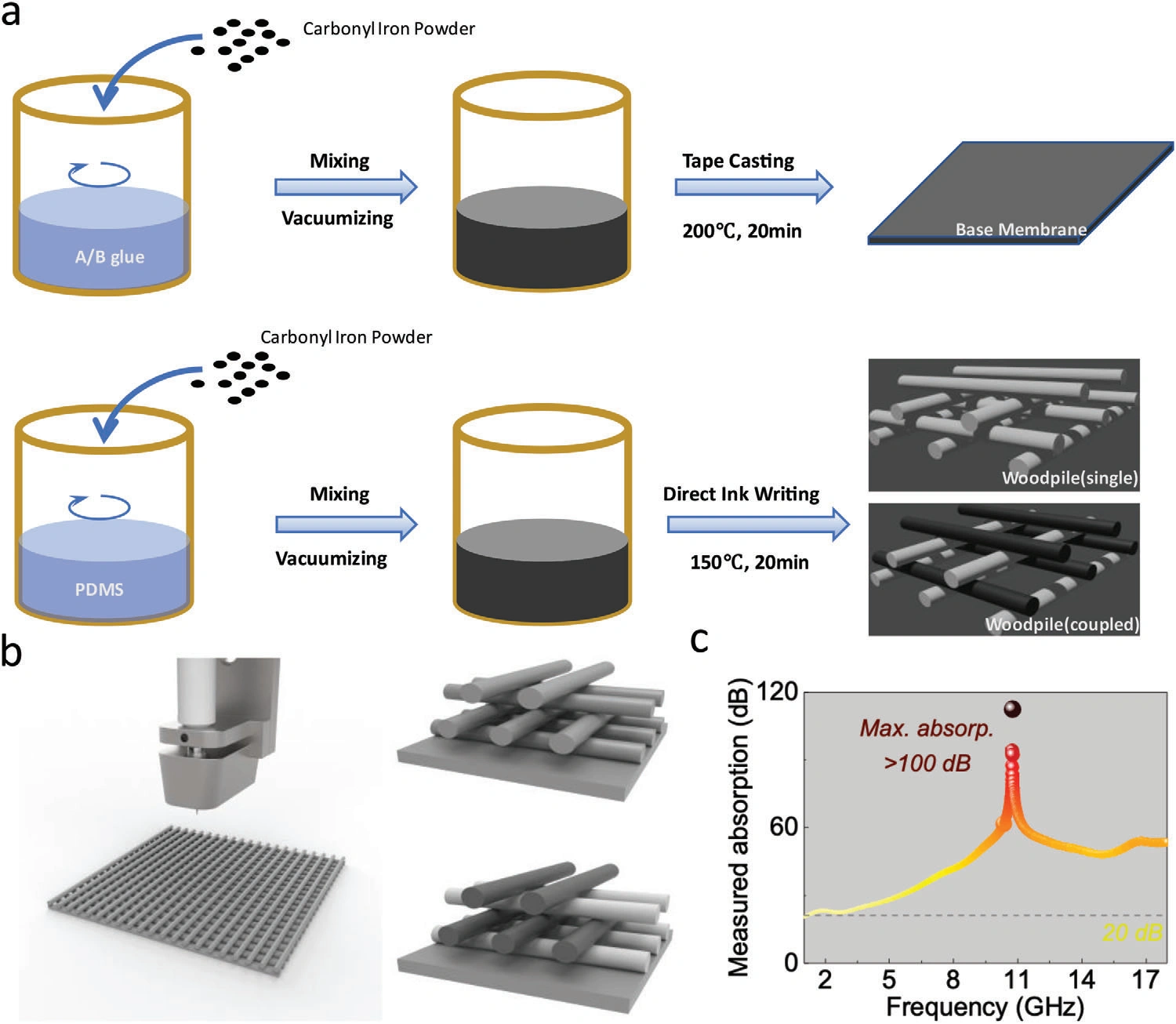
△ Figure 1, a schematic diagram of the manufacturing process illustrates (a) the manufacturing process of BM and 3D WP photonic crystals. High frequency CIP was mixed with silicone elastomer to generate tape casting precursor for BM (bottom row) or direct ink writing for WP (top row). Coupling WP was written using two CIP concentrations between each layer. (B) Layer-by-layer printing of 3D WP photonic crystals(Adventure Technology Direct Writing DIW 3D Printing Equipment (Model ADT-3D-LB-Printer-0050))Schematic diagram. The monolithic absorber includes the integration of the BM with a single WP or coupled WP. (c) The maximum absorption of the BM-coupled WP integrated absorber exceeds 100 dB at 10.76 GHz. BMs containing 89%, 87%, 85%, 83% and 80% CIP were defined as 89 BM, 87 BM, 85 BM, 83 BM and 80 BM, respectively. A single WP contains 10%, 20%, 30%, and 40% CIP, which are defined as 10WP, 20WP, 30WP, and 40WP, respectively. Coupling WP contains 10% and 20%, 10% and 30%, 10% and 40%, 20% and 30%, 20% and 40%, 30% and 40% CIP, defined as 10/20WP, 10/30WP, 10/40WP, 20/30WP, 20/40WP, 30/40WP, respectively.
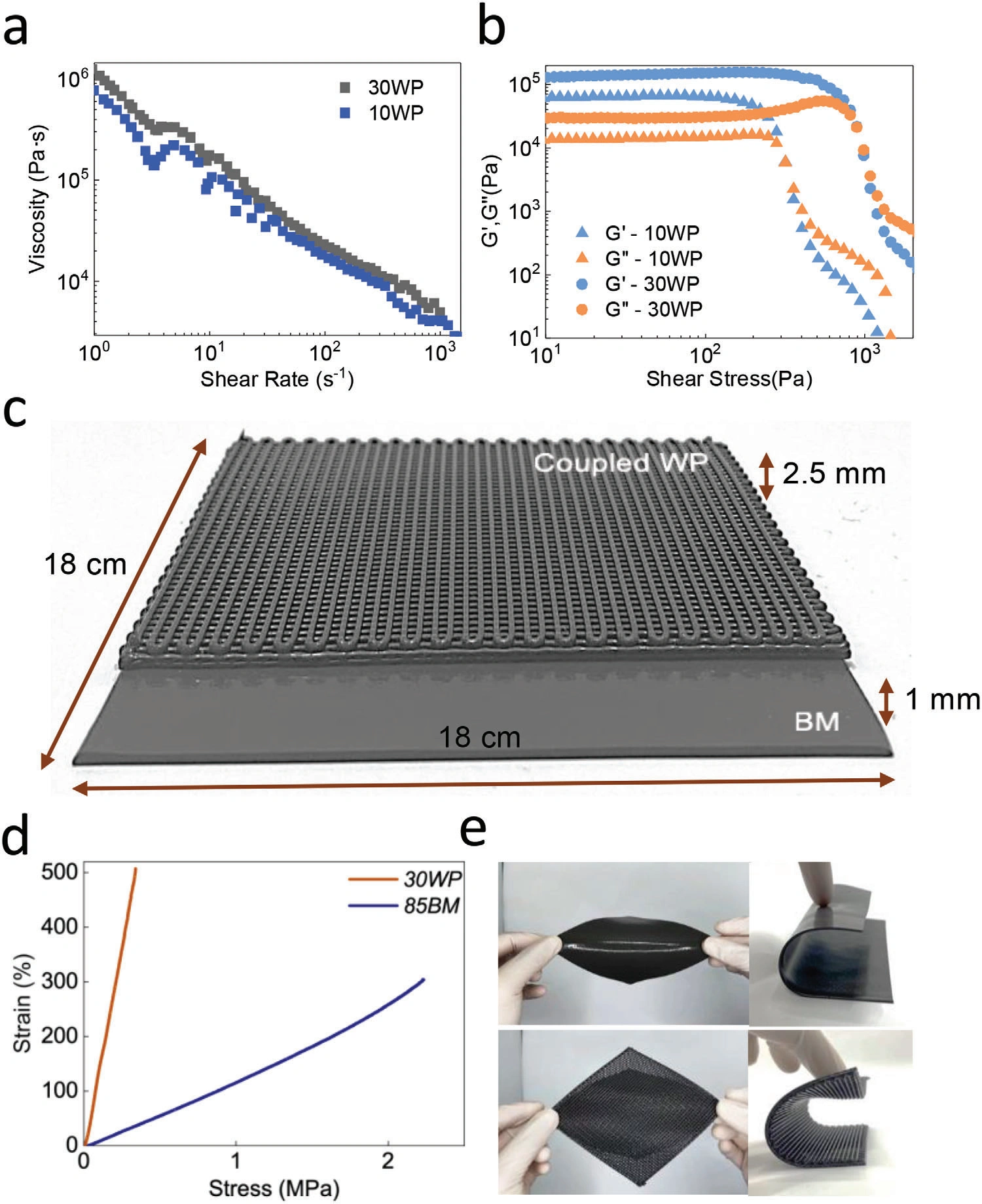
△ Figure 2, the characteristics of wave absorption BM and 3D WP materials (a) The relationship between the apparent viscosity of 10WP and 30WP composite inks and the shear rate. (B) Changes in elastic modulus (G') and viscoelastic modulus (G'') of 10WP and 30WP composite inks with applied shear stress. (C) The image of the manufactured BM-coupled WP integrated microwave 3D absorber and the geometric characteristics (thickness and size) of the WP. (D) Mechanical properties of 85 BM and 30WP when force is applied to break tension. (e) Flexibility of BM and 3D WP photonic crystals.
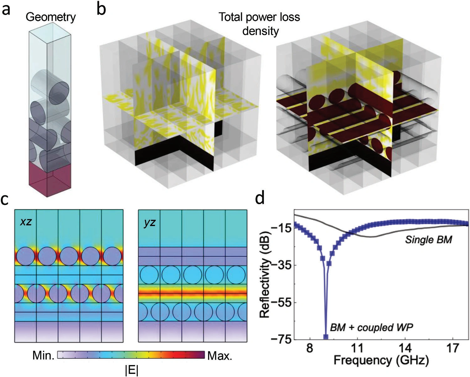
△ Figure 3, Electromagnetic simulation of integrated microwave absorber (a) Geometric layout. The top four-layer cylinder is a 3D coupled 10/40WP photonic crystal, and the bottom layer is 85 BM. (B) Simulated total power loss density distribution of a system containing only BM and an integral absorber containing BM and coupled WP. (C) The electric field distribution shows the resonance of the WP photonic crystal at 9 GHz. (d) Simulated reflectance spectra of BM and integral absorber consisting of BM and WP.
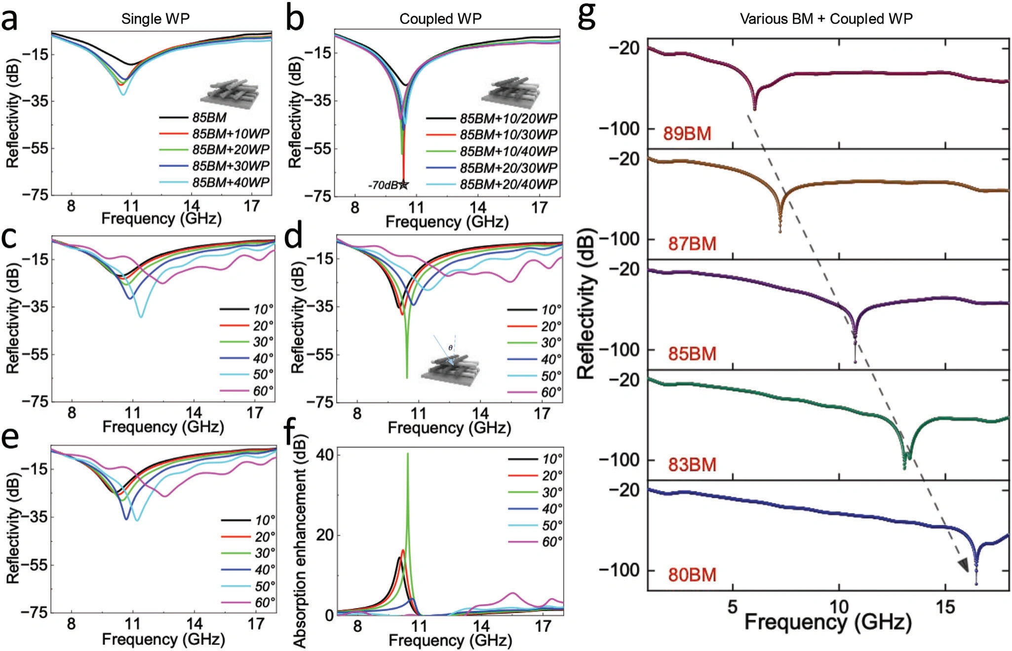
Figure 4, Reflectance of microwave absorber (a) BM made of a single WP with different CIP concentrations. (B) Coupling WP and BM for different concentration pairs. The mass fraction of all BM was 85%. The reflectance spectra are as follows:(c) 85 BM vs. 10WP,(d) 85 BM vs. 10/30WP,(e) 85 BM vs. 30WP, and the behavior of 85 BM vs. 30WP = 10 °, 20 °, 30 °, 40 °, 50 °, and 60 °. (f) Absorption enhancement of BM-10/30WP absorber and BM-10WP or BM-30WP absorber at different angles. (G) By adjusting the concentration of BM from 89% to 80%, the resonance frequency was engineered from 6 GHz to 16.5 GHz.
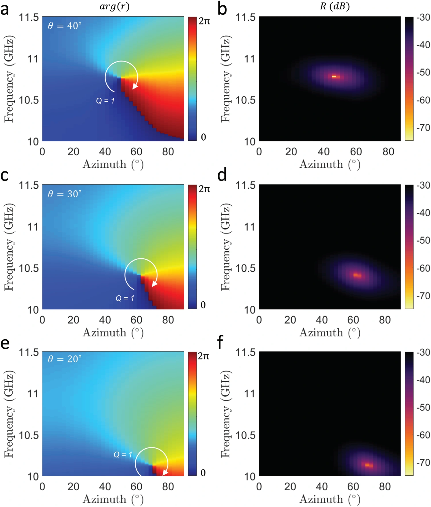
△Figure 5, the reflection singularity and topological charge caused by the perfect absorption measured experimentally, in the parameter space of frequency and azimuth, (a, c, e) reflection phase and (B, d, f) reflection amplitude are for different incidence Elevation angles (40 °, 30 ° and 20 ° from top to bottom) are measured. The topological charge shows that the coupling WP is robust to the disorder of the parameters.
Conclusion
An integrated base film and DIW printing3D Wooden Pile Photonic Crystal Microwave Absorber. The3D AbsorberWith good flexibility, largeabsorption bandwidth, andabsorption singularityinducedtopological charge. After the internal microwave enters the absorber, it passes throughmagnetic lossandresonance dissipationAchieve absorption. Through willWPIntegrated with BM, at all tested incident angles (ranging from 10 ° to 60 °), the effective range with an absorption bandwidth higher than 90% extends to about10 GHz. The range of specific absorption bands in the BMCIP concentrationclosely related, which means that the CIP concentration can be controlled and adjusted to manufactureDesigns Absorption Bandofengineering absorber. Compared to the BM of a single WP,Coupled WPsignificantly enhanced throughResonance-enhanced microwave-matter interactionAbsorption of waves. Furthermore, the coupling of WP throughrobustness of topological chargeprotected.Perfect absorption point, to ensure that it does not disappear, to achieve a consistentPerfect absorption.