
As electronic devices become increasingly compact and semiconductor manufacturing processes continue to advance, the demand for high-performance ceramic components is growing rapidly. Components used in wafer handling systems, electrical insulation assemblies, vacuum environments, and electronic packaging must combine dimensional precision with excellent thermal and electrical properties.
Among advanced engineering ceramics, Alumina (Al₂O₃) remains one of the most widely used materials due to its high electrical resistivity (>10¹⁴ Ω·cm), dielectric strength (>10 kV/mm), excellent corrosion resistance, and long-term thermal stability. However, manufacturing complex alumina components through conventional methods often presents significant challenges. Features such as internal channels, thin walls, threaded structures, and lightweight lattice geometries typically require expensive tooling or extensive post-machining, increasing both cost and lead time.
To overcome these limitations, ADT fabricated a series of alumina ceramic components using its DLP ceramic 3D printing technology. By combining high-resolution photopolymerization with ceramic-filled slurries, the process enables the production of complex ceramic geometries directly from CAD models, significantly reducing design constraints while accelerating development cycles.
Alumina Vacuum Chuck for Semiconductor Wafer Handling
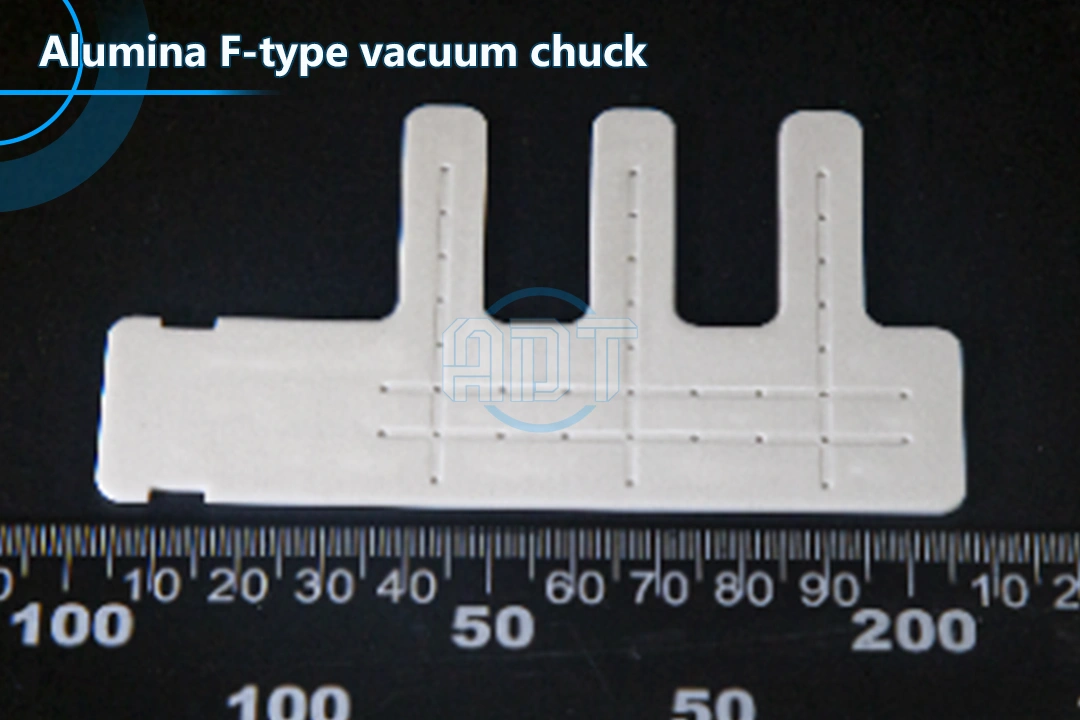
Vacuum chucks play a critical role in semiconductor wafer transportation, positioning, and processing. Their performance depends heavily on flatness, vacuum uniformity, and the accuracy of internal flow pathways.
The alumina vacuum chuck shown here incorporates a network of fine vacuum channels and uniformly distributed suction holes that were manufactured as an integrated structure through DLP ceramic 3D printing. Producing similar geometries using conventional machining would require multiple fabrication and assembly steps, introducing additional tolerances and potential failure points.
By fabricating the component directly from a digital model, the design can be rapidly modified and optimized during R&D activities, making it particularly suitable for semiconductor equipment development and laboratory-scale process validation.
Lightweight Honeycomb Insulating Structure
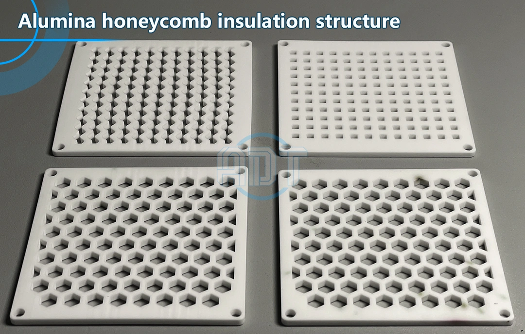
Advanced electronic and power systems frequently require insulating components that combine low weight with high structural rigidity. Honeycomb structures offer an excellent strength-to-weight ratio but are notoriously difficult to manufacture in ceramic materials using traditional processing techniques.
Through ceramic additive manufacturing, fine and highly uniform honeycomb geometries can be produced without dedicated tooling. The resulting structure maintains the excellent dielectric properties of alumina while reducing overall material usage and component weight.
Researchers are increasingly exploring honeycomb structures for thermal management systems, high-temperature insulation, aerospace electronics, and advanced electronic packaging applications where both thermal stability and lightweight design are essential.
Threaded Alumina Insulating Sleeve
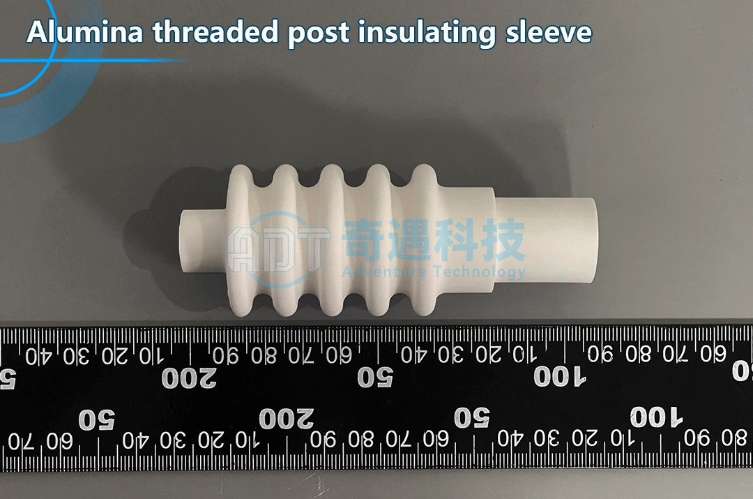
Threaded ceramic components are commonly used in high-voltage systems, vacuum devices, and specialized laboratory equipment. However, machining threads into sintered ceramics is often associated with tool wear, chipping, and low manufacturing yields.
Using DLP ceramic 3D printing, both internal and external thread features can be integrated directly into the printed geometry. The resulting alumina insulating sleeve exhibits well-defined thread profiles and consistent dimensional accuracy while minimizing the risk of machining-induced defects.
This design freedom enables engineers and researchers to incorporate ceramic fastening and insulation features into devices that would otherwise be difficult or uneconomical to manufacture.
Circular Alumina Connector Housing
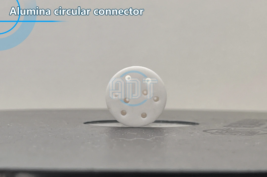
Electrical connectors operating in demanding environments require exceptional insulation performance, dimensional stability, and long-term reliability. Alumina ceramics are particularly attractive for these applications because of their high dielectric strength and resistance to electrical degradation.
The circular connector housing presented in this project features multiple precision-aligned pin openings within a compact geometry. Through DLP ceramic 3D printing, the component was produced as a single integrated structure, eliminating many of the alignment challenges commonly associated with conventional fabrication methods.
For applications such as aerospace electronics, vacuum instrumentation, semiconductor equipment, and high-density electrical interconnects, ceramic additive manufacturing provides a practical route to producing customized ceramic connector designs with reduced development time.
Accelerating Research and Prototype Development
For many research laboratories and engineering teams, the greatest barrier to innovation is not design capability but manufacturing flexibility. Traditional ceramic fabrication often requires dedicated molds, long lead times, and significant upfront investment, making rapid iteration difficult.
DLP ceramic 3D printing addresses this challenge by enabling tool-free production of complex alumina ceramic components directly from digital designs. Features such as internal channels, thin walls, lattice structures, customized mounting interfaces, and threaded geometries can be incorporated without increasing tooling complexity.
As a result, researchers can evaluate multiple design iterations within a significantly shorter development cycle, accelerating experimental validation and supporting rapid prototyping workflows.
Whether developing semiconductor process equipment, high-voltage insulation systems, vacuum-compatible components, or next-generation electronic devices, ceramic additive manufacturing provides new opportunities to explore designs that were previously difficult or impossible to realize using conventional ceramic processing methods.
Looking to Develop Custom Alumina Ceramic Components?
ADT specializes in DLP ceramic 3D printing solutions for universities, research institutes, and industrial R&D teams. From material evaluation and design optimization to prototype fabrication and small-batch production, we help researchers transform complex ceramic concepts into functional components.
Contact our engineering team to discuss your next alumina ceramic project and explore how ceramic additive manufacturing can accelerate your research.
(If you would like to know the exact test parameters for the printed examples in the article, please contact us.)