
Industry Insights
Recently, the team led by Zhou Guoxiang from Harbin Institute of Technology published a study titled 'Conformal and rapid micro-molding manufacturing of ultraviolet-curable silver paste on curved surfaces using digital light processing' in the Journal of Materials Science & Technology. This research achieved rapid micro-molding of silver paste on curved surfaces using Digital Light Processing (DLP) technology, addressing the limitations of traditional manufacturing processes in complex surfaces and fine structures.
Original link: https://doi.org/10.1016/j.jmst.2024.06.039
Adventure Technology official website: https://www.adventuretech.cn/
If you cannot open it, please copy the URL to your browser for reference.
Research Content
Background of Silver Paste Application:Silver paste is a conductive material commonly used in the manufacturing of electronic devices, especially as a conductive medium in electronic components. Due to its excellent conductivity, silver paste is widely used in solar cells, sensors, and other microelectronic devices. Traditionally, silver paste is usually formed through methods such as screen printing, but these methods have certain limitations in manufacturing precision and application on complex surfaces, especially in meeting high precision and high efficiency requirements.
Digital Light Processing Technology (DLP):DLP is an advanced 3D printing technology that achieves object formation by layer-by-layer curing of liquid photosensitive resin through digital light projection. Unlike traditional stereolithography (SLA) or selective laser sintering (SLS) technologies, DLP technology uses light projection as the curing source, allowing for rapid curing of larger areas in a shorter time, thus providing higher forming precision and greater production efficiency.
Research Objectives:The objective of this paper is to explore how to utilize DLP technology to achieve efficient manufacturing of photopolymerized metal circuits on flat and curved substrates, thereby addressing the issues of rapid curing and controllable sintering of photopolymerized metal pastes. By precisely controlling the line width and curing depth of the photopolymerized circuits, this research not only improves the precision of circuit manufacturing but also significantly enhances the applicability and versatility of photopolymerized circuit technology on complex substrates.
The following are the research methods and data from the article:
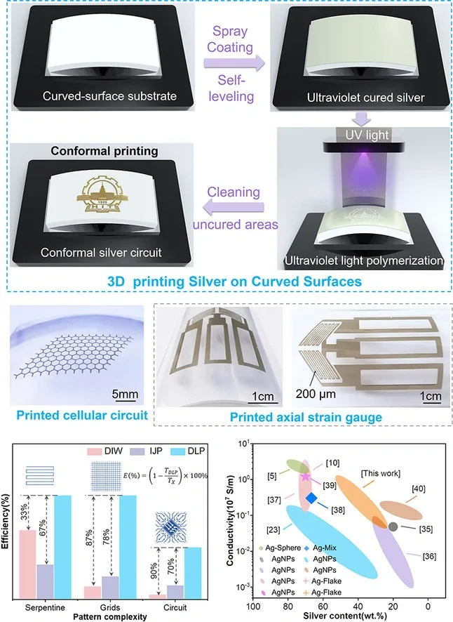
△ Figure 1, Illustration and demonstration of DLP printed circuits: (a) Silver-based circuit printing process. (b) Silver-based circuit on curved surfaces. (c) Efficiency comparison of different printing methods. (d) Electrical performance compared to other printing methods.
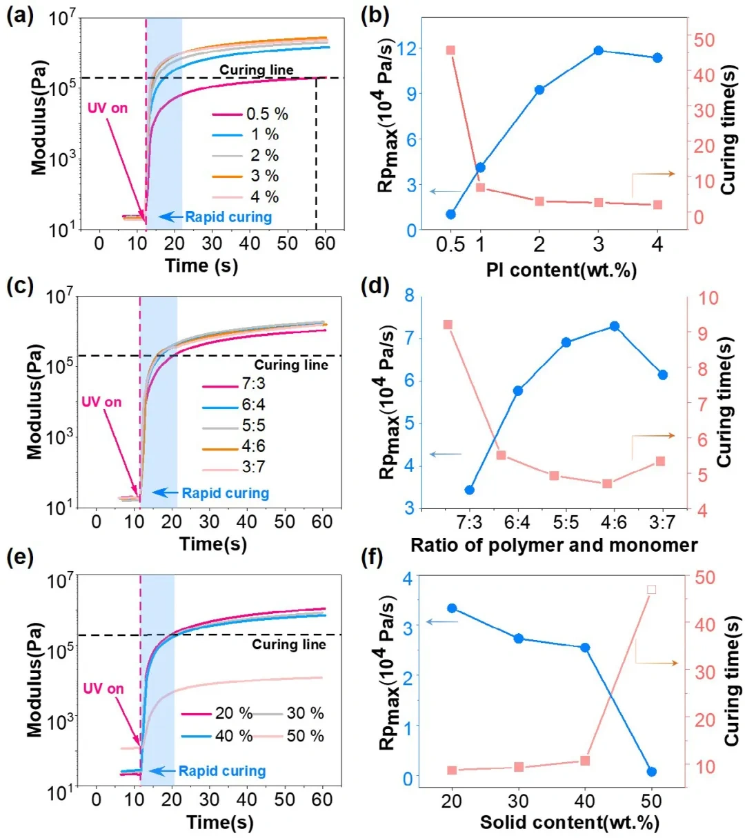
△ Figure 2, Characterization of curing properties of ultraviolet-curable silver paste (UV-SPs): (a, c, e) Modulus changes of UV-curable silver paste under radiation exposure with different photoinitiator contents, resin ratios, and solid contents. (b, d, f) Maximum polymerization rate and curing time.
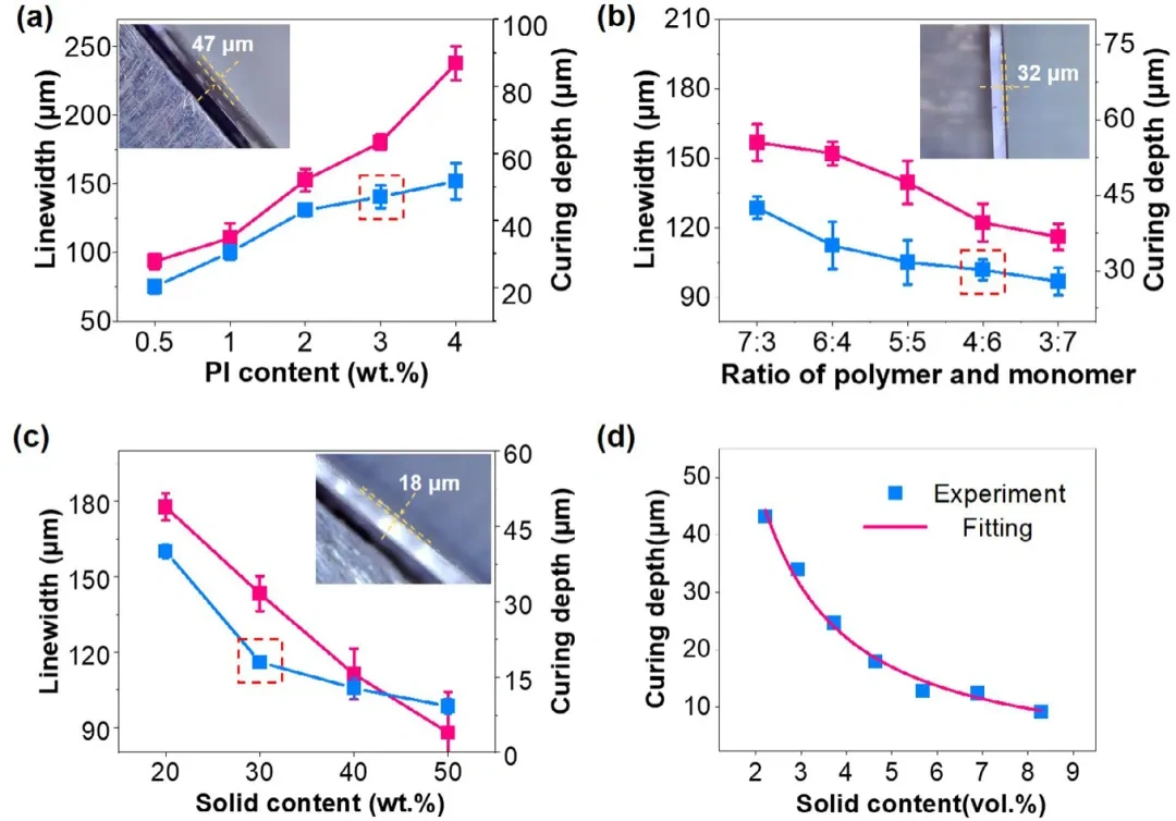
△ Figure 3, Forming characteristics of ultraviolet-curable silver paste (UV-SPs): (a, b, c) Line width (pink) and curing depth (blue) of UV-curable silver paste under different photoinitiator contents, resin ratios, and solid contents. (The inset shows optical micrographs of the curing depth in the red box). (d) Volume fraction of solid content versus curing depth and fitting curve.
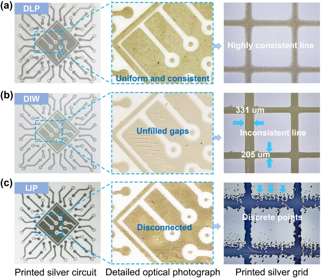
△ Figure 4, (a) DLP, (b) DIW, and (c) IJP printed micrographs.
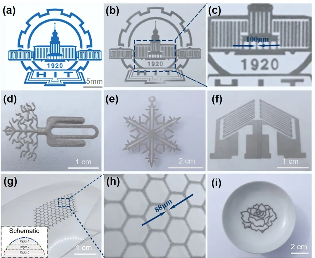
△ Figure 5, Surface forming demonstration of ultraviolet-curable silver paste (UV-SP): (a) Harbin Institute of Technology logo design. (b–f) Flat circuits printed on different substrates (b, d, e, and f are glass, metal, plastic, and ceramic substrates, respectively). (g–i) Curved circuits printed on different substrates (g and i are plastic and ceramic substrates), with an inset showing a schematic of conformal surfaces.
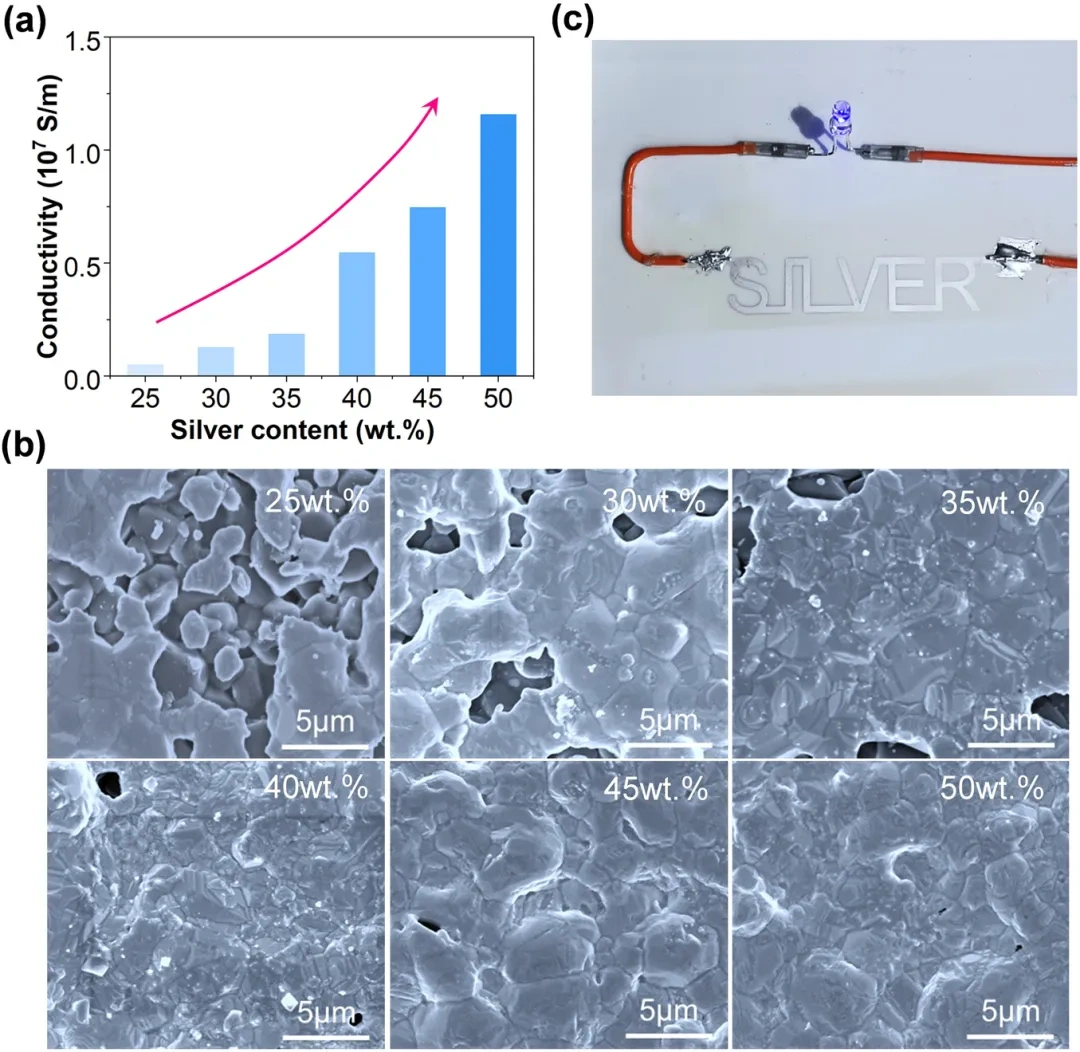
△ Figure 6, Electrical performance of photopolymerized conductive circuits: (a) Conductivity at different solid contents. (b) Scanning electron microscope (SEM) images at different solid contents. (c) Conductivity display of 30wt.% UV-SP printed circuits.
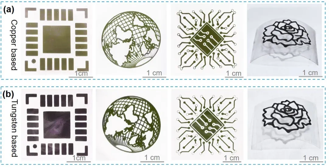
△ Figure 7, Images of electronic pastes printed using DLP technology: (a) Copper-based circuit and (b) Tungsten-based circuit.
Conclusion
This research proposes a new method for rapid manufacturing of photopolymerized metal paste circuits on flat and curved substrates usingDigital Light Processing (DLP) technology.This method significantly improvesmold efficiencyespecially in the manufacturing ofcomplex circuit patterns.By adjusting the ratio of photosensitive materials and conductive fillers, it is possible to achievea printing line width of 88 μmandcontrollable curing depths from 10 μm to 53 μm.The study shows that in theUV-SP material system,using2% photoinitiator concentrationcan optimize forming performance and improve curing efficiency. The 2D and 3D circuits made using this method exhibit goodadhesionandstability in electrical performance,with conductivity approaching the theoretical conductivity of metals (1.16 × 10⁷ S/mand). Additionally, this method can also be applied to other metal conductive pastes such ascopperandtungsten,solving the issues of low precision and complex programming surface fitting problems in traditionalandIJP methods.等其他金属导电浆料,解决了传统DIWandIJP方法的低精度with conductivity approaching the theoretical conductivity of metals (复杂编程and表面贴合问题This technology not only shortensthe circuit preparation timebut can also be used to manufacturecomplex curved circuitssuitable forflexible electronicswith conductivity approaching the theoretical conductivity of metals (curved circuitsandand multilayer electronic devicesapplications.