
Knowledge Interpretation
As semiconductor technology advances at a breakneck pace, the demands for materials in integrated circuits (ICs), microelectronic devices, sensors, and other cutting-edge fields have escalated significantly. Among these materials, ceramics have emerged as increasingly vital due to their exceptional high-temperature resistance, corrosion resistance, electrical insulation, and mechanical strength. The continuous breakthroughs in additive manufacturing, particularly 3D printing, have ushered in new opportunities for the application of ceramics in the semiconductor industry. This article will delve into the innovative applications of ceramic 3D printing in the semiconductor sector and the technological revolution it has brought about.
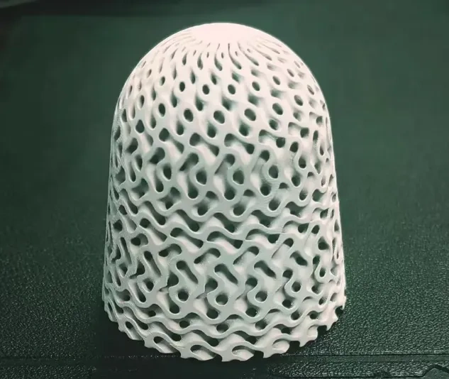
△ Figure 1. Silicon nitride ceramics. (Source: Internet, please delete if infringed)
The Importance of Ceramic Materials in Semiconductors
Ceramic materials have established a significant presence in the semiconductor industry due to their unique properties. Common ceramics, such as alumina (Al₂O₃), zirconia (ZrO₂), and silicon nitride (Si₃N₄), are widely used in various critical components of semiconductor manufacturing, including:
Thermal Management Components: High-power operation of semiconductor devices generates substantial heat. The excellent thermal conductivity of ceramics effectively addresses the cooling challenges in high-power semiconductor equipment.
Electrical Insulation Materials: Ceramics exhibit superior electrical insulation properties, making them widely used in semiconductor packaging and isolation components to ensure the proper functioning of electronic devices.
High-Temperature Components: Many semiconductor manufacturing processes require high-temperature environments. The high-temperature tolerance of ceramics makes them ideal for applications such as wafer processing and thin-film deposition.
However, traditional ceramic processing methods are fraught with limitations, such as low manufacturing precision, long production cycles, and poor design flexibility, which have constrained the broader application of ceramic materials in the semiconductor industry.
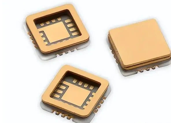
△ Figure 2. Ceramic packaged semiconductor. (Source: Internet, please delete if infringed)
Ceramic 3D Printing Overcomes Traditional Manufacturing Bottlenecks
The introduction of 3D printing technology has revolutionized the application of ceramic materials by overcoming the limitations of traditional manufacturing methods. In the semiconductor industry, ceramic 3D printing offers several advantages that are unattainable through conventional manufacturing processes:
High-Precision Manufacturing: 3D printing technologies, particularly Digital Light Processing (DLP) and Stereolithography (SLA), can achieve micron-level precision, meeting the semiconductor industry's stringent requirements for dimensional accuracy and complex structures.
Rapid Prototyping: Traditional ceramic manufacturing typically involves time-consuming mold-making and high-temperature sintering. In contrast, 3D printing enables the rapid production of high-precision ceramic components and allows for iterative optimization, significantly reducing product development cycles.
Complex Geometry Printing: 3D printing can easily create complex geometries and fine structures that are difficult or impossible to achieve with traditional methods. For microchannels, microstructures, and integrated circuit components in the semiconductor industry, 3D printing offers unprecedented design freedom.
Material Customization: Ceramic 3D printing supports customized material formulations, allowing the composition and properties of the ceramic to be tailored to meet the specific requirements of semiconductor devices. This ensures that ceramic components are optimized for their intended applications.
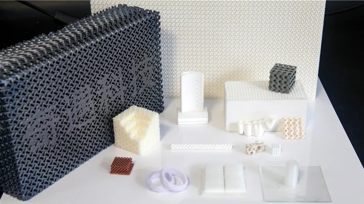
△Figure 3. Porous ceramic samples printed by Adventure Technology Ceramics 3D.
Innovative Applications of Ceramic 3D Printing in the Semiconductor Industry
As 3D printing technology continues to mature, an increasing number of semiconductor companies are leveraging it for the manufacturing of critical components, achieving remarkable results.
Semiconductor Packaging and Thermal Management Solutions
During the semiconductor packaging process, ceramic materials are often employed for electrical insulation and thermal management. Traditional packaging techniques typically rely on aluminum or silicon materials, which exhibit poor thermal management capabilities under high-temperature and high-power-density conditions. This limitation restricts the performance enhancement of electronic devices. In contrast, ceramic 3D printing offers superior thermal conductivity and electrical insulation, especially in high-power microelectronic devices and power semiconductors. Ceramic 3D-printed packaging provides enhanced thermal dissipation, ensuring stable device operation at elevated temperatures.
For instance, 3D-printed silicon nitride (Si₃N₄) ceramic materials can effectively dissipate heat under extreme conditions. They are widely used in the packaging and thermal management systems of high-power lasers, LED devices, and high-frequency electronic equipment.
Precision Structures in Microelectronic Devices
3D printing technology is capable of fabricating complex structures at the micron and even nanometer scale, making it highly suitable for the research and development as well as the manufacturing of microelectronic devices. For example, in integrated circuit (IC) manufacturing, extremely fine microchannels and microstructures are required to facilitate the conduction of electric current and the dissipation of heat. With 3D printing, these intricate microstructures, which are difficult to achieve with conventional machining methods, can be accurately printed, thereby offering higher performance and smaller form factors for semiconductor devices.
For example, ceramic 3D printing can be used to create microfluidic channels. These channels can be employed for chip cooling, chemical reactors, and sensor development, significantly enhancing the precision and efficiency of semiconductor devices.
Customized Molds and Tools in Semiconductor Manufacturing
The semiconductor industry has extremely high demands for molds and manufacturing tools. Traditional ceramic manufacturing methods often fail to meet these requirements, especially for small-batch and customized production. Ceramic 3D printing provides a flexible solution. Through 3D printing technology, complex and precise molds can be rapidly produced for processes such as semiconductor wafer processing, laser etching, and the fabrication of micro- and nanostructures. This approach reduces production cycles and costs.
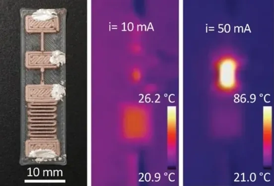
△ Figure 4. Ceramic 3D printing device and thermal conductivity visualization imaging. (Image source: Internet, please delete if infringed)
Challenges and Prospects of Ceramic 3D Printing
Despite the promising applications of ceramic 3D printing in the semiconductor industry, several challenges remain. First, the material systems and process technologies for ceramic 3D printing are still evolving. Enhancing printing speed, reducing costs, and improving the reliability and stability of the final products are key priorities for current technological advancements. Second, the sintering processes and the physical properties of the finished products need further optimization to ensure that they meet the semiconductor industry's stringent requirements for high-temperature resistance, mechanical strength, and electrical performance.
However, with continuous advancements in 3D printing technology, the application of ceramic materials in the semiconductor industry is set to expand significantly. In the future, ceramic 3D printing is expected to move beyond high-end customization and small-scale production to enter the realm of large-scale manufacturing. This shift will bring about more innovation and breakthroughs in the semiconductor industry.