
Reduced Photopolymerization Ceramic 3D Print of EM-Absorbing SiBCN Metamaterials
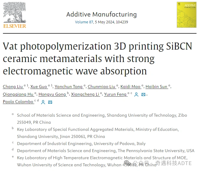
Recently, a team led by Yurun Feng from Shandong University of Technology published a study titled Vat photopolymerization 3D printing SiBCN ceramic metamaterials with strong electromagnetic wave absorption in Additive Manufacturing.
Using ceramic precursor polymer as raw material, using photopolymerization technology, SiBCN polymer-derived ceramic metamaterials with structure and function were obtained.
Original link: https://www.sciencedirect.com/science/article/abs/pii/S2214860424002859
Ceramic 3D Printing Meets SiBCN Metamaterials
In recent years, driven by the evolution of 5G networks, radar technology, and stealth systems, the demand for high-performance electromagnetic wave (EMW) absorbing materials has risen sharply. Among the promising candidates are polymer-derived ceramics (PDCs), especially SiBCN ceramics.
Yet, few studies have combined ceramic 3D print techniques with SiBCN to produce metamaterials. This new research bridges that gap by using Ceramic 3D Printing via DLP (Digital Light Processing) to fabricate low-density triple periodic minimal surface (TPMS) lattice structures.
Ceramic 3D Print Fabrication Process
1. Schematic of the DLP-SiBCN ceramic metamaterial manufacturing process.
Three Structural Forms Compared
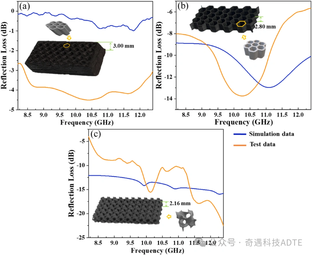
2. CST simulation vs test results: Oblique honeycomb, hexagon honeycomb, and gyroid structures.
Material Characterization and Ceramic Structure
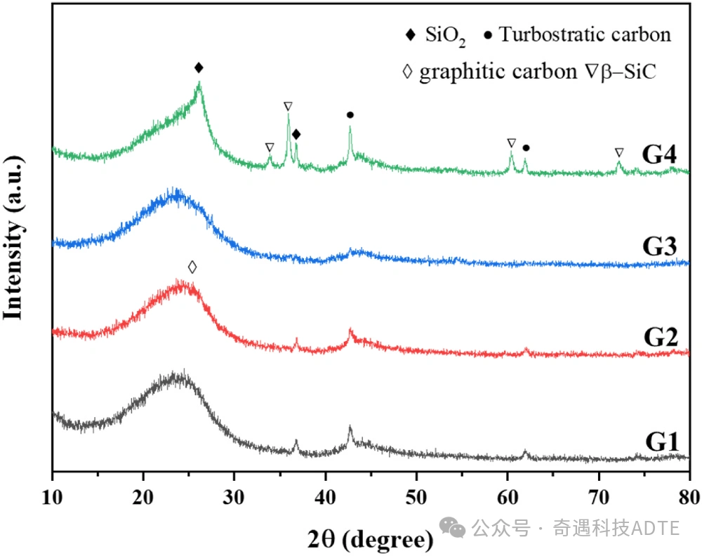
3. X-ray diffraction spectrum of DLP-SiBCN ceramic showing formation of β-SiC and graphitic carbon.
Microstructure After Pyrolysis
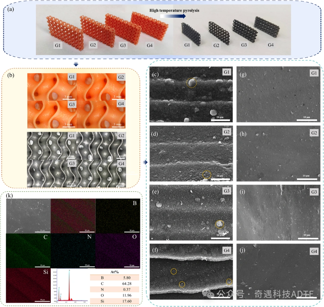
4. SEM images of surface and cross-section of pyrolyzed ceramics.
High-Temperature Structural Integrity
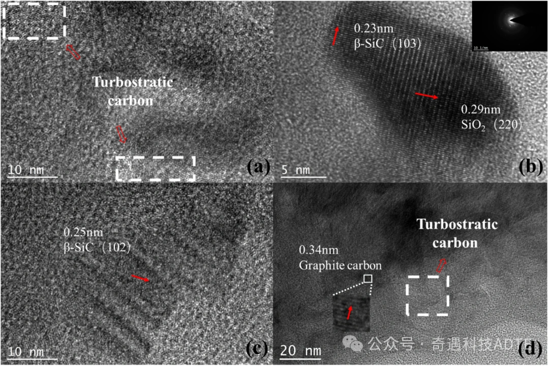
5. Transmission electron microscopy of G2 samples at 1200 °C, showing fine ceramic phase development.
Thermal, Mechanical & Electrical Performance
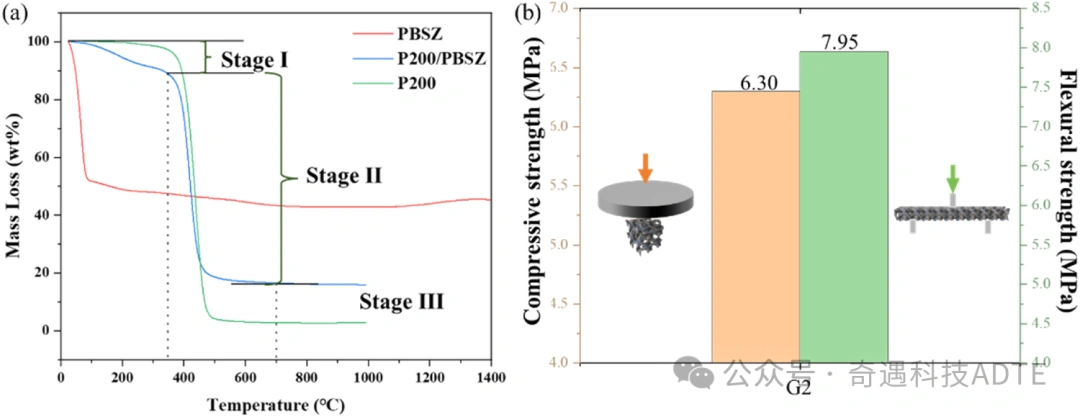
6. TGA and compression strength test reveal G2’s high ceramic yield and mechanical performance.
Surface Composition
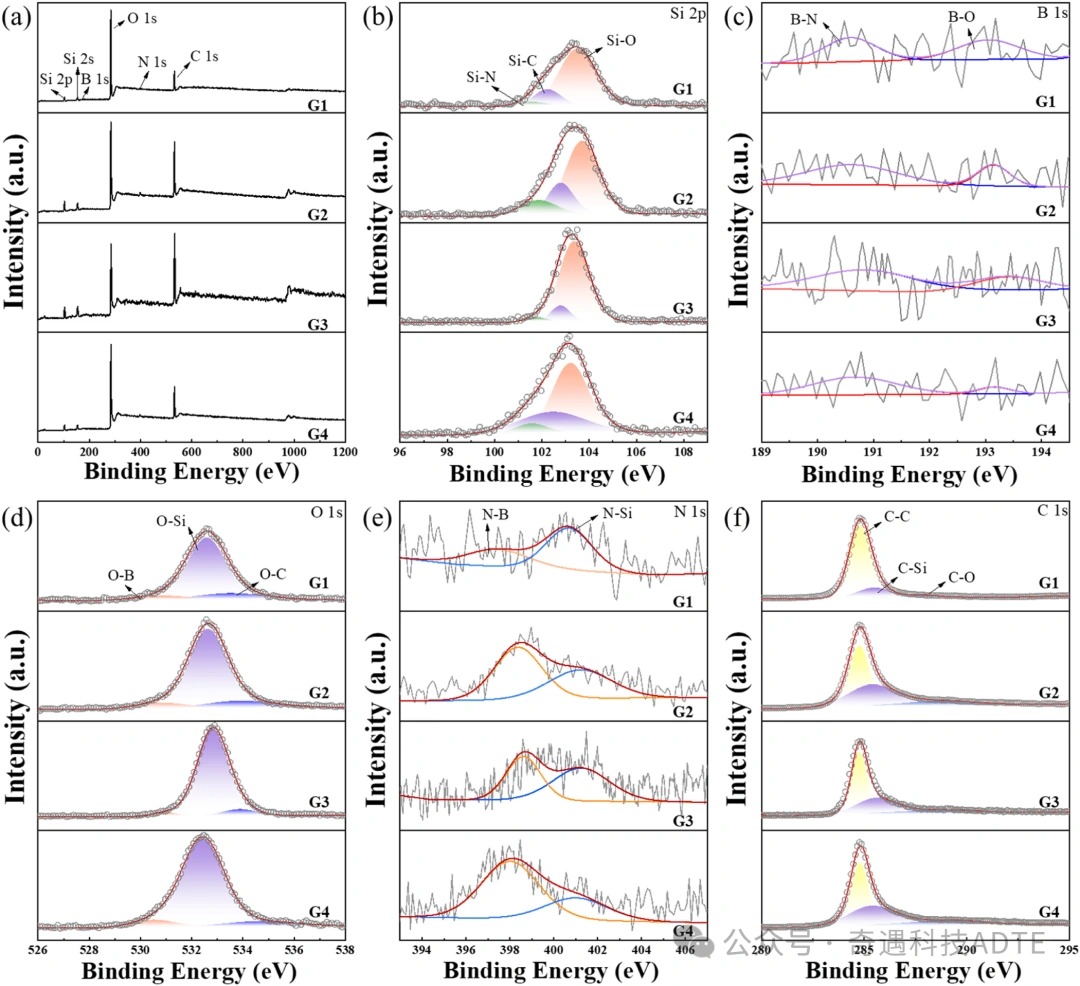
7. XPS spectra showing elemental bonds: Si, B, C, N, O.
Raman Analysis & Dielectric Properties
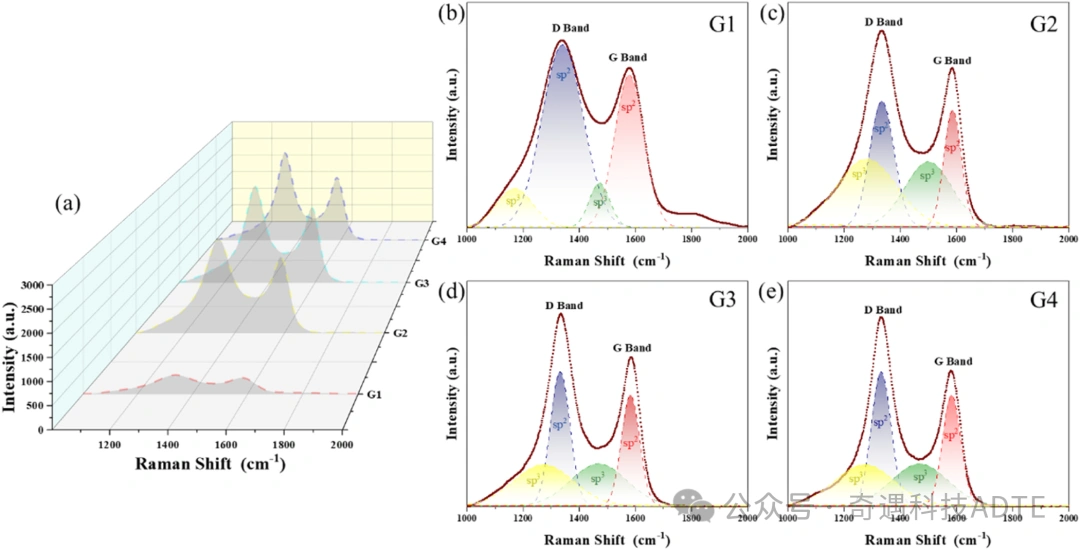
8. Raman shift confirms carbon phase evolution across temperature sets.
EMW Absorption & Impedance Matching
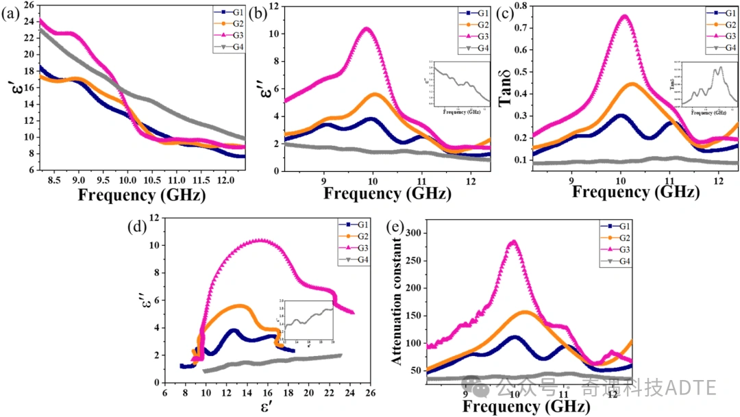
9. Dielectric constant measurements showing tunable EM response.
10–13. Matching |Zin/Z0| curves and reflection loss across temperature groups.
Metamaterial Absorption Mechanism and Performance
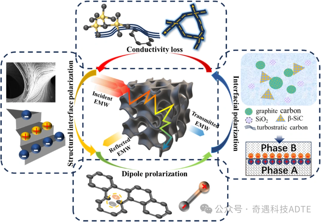
15. Gyroid metamaterial EM absorption schematic based on ceramic 3D print geometry.
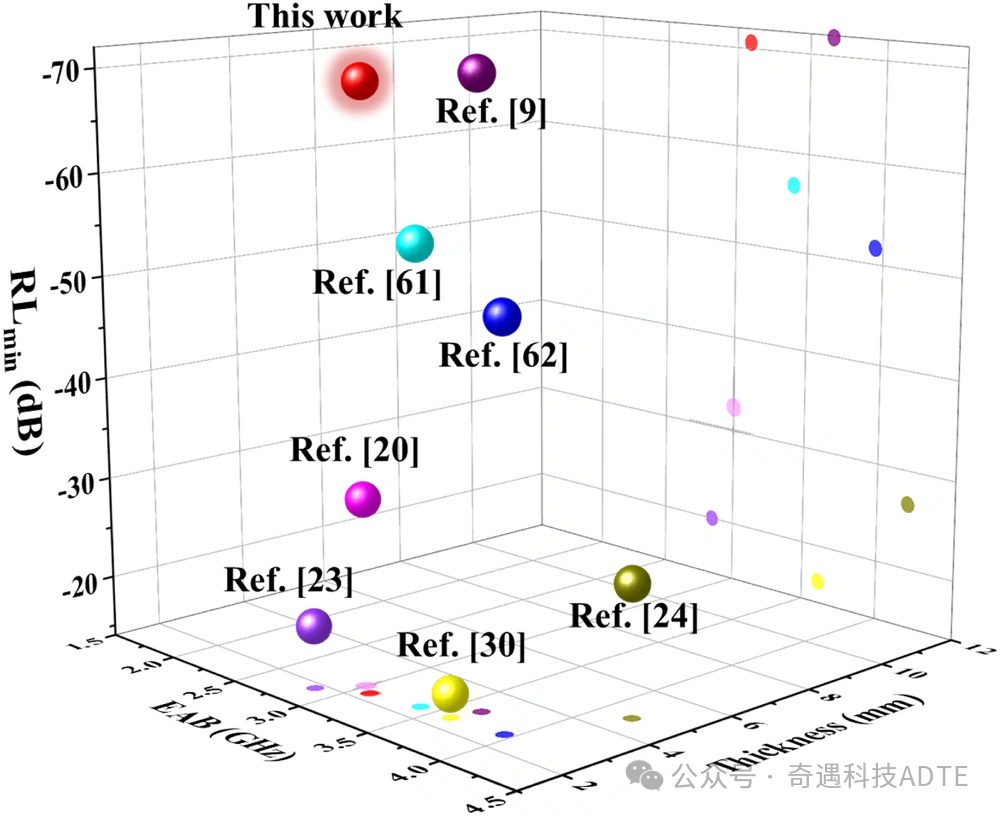
16. Sample G2 outperforms literature-reported materials in EM absorption strength and bandwidth.
Conclusion: What Ceramic 3D Printing Enables
Ceramic 3D Print allows precise TPMS structures that boost EM reflection and internal absorption.
Pyrolysis temperature tuning creates β-SiC and carbon nanostructures, enhancing conductivity and dielectric loss.
DLP-printed SiBCN metamaterials offer top-tier EMW absorbing properties for aerospace and defense.
This ceramic 3D printing technology shows strong potential in harsh environment integration of structure and function.
Ceramic 3D Printing: The Future of Electromagnetic Engineering
Reduced photopolymerization in ceramic 3D print processes leads to lower porosity, better material control, and repeatable high-performance EM shielding metamaterials. Ceramic 3D Printing is no longer just a lab concept—it’s enabling real-world defense, aerospace, and telecommunication advancements today.