
How Ceramic 3D Printing Is Revolutionizing Electronics and Semiconductor Packaging
When we talk about semiconductors and electronics, most people think about silicon wafers, cleanrooms, and microchips. But behind the scenes, there’s a critical component often overlooked: the packaging. That’s where ceramic 3D printing is quietly driving a revolution—especially for high-performance and high-frequency electronic systems.
1. Thermal Management Gets a Boost
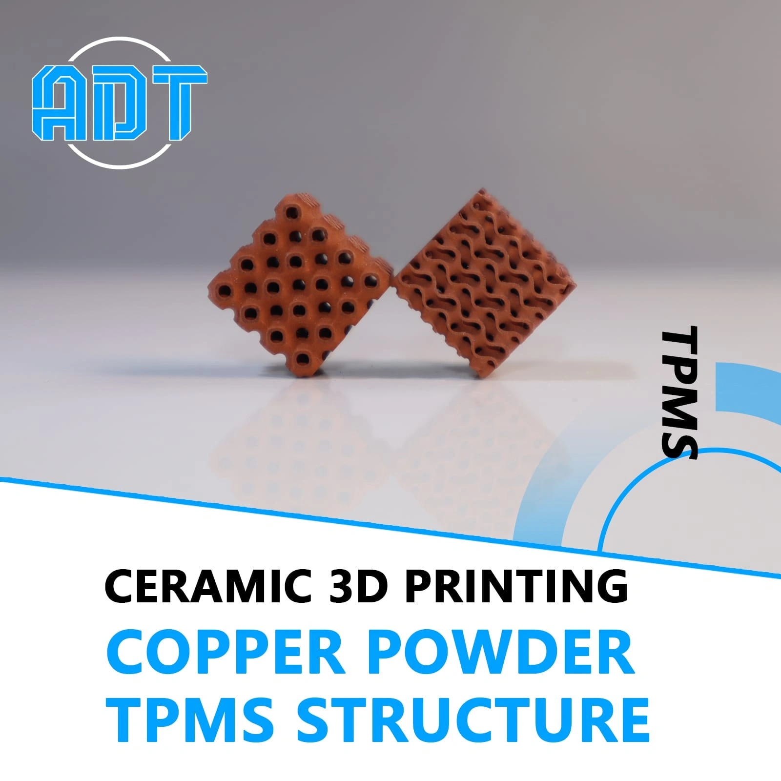
Modern chips generate a lot of heat. Traditional plastic packaging materials simply can’t keep up. High thermal conductivity ceramics like alumina and aluminum nitride are essential for dissipating heat in power modules, RF devices, and laser systems. With DLP ceramic 3D printing, engineers can now design intricate heat-dissipation geometries—such as TPMS lattice structures—that were previously impossible to fabricate using traditional methods.
2. Enabling 3D Circuit Integration
As electronics shrink, designers need to think vertically. Ceramic 3D printing allows us to produce multi-layered, multi-material substrates with embedded vias and cavities for embedded components. This is particularly useful in system-in-package (SiP) and advanced IC integration applications, where space and performance matter equally.
3. High-Frequency and High-Voltage Reliability
In high-frequency communication systems, dielectric properties of materials are critical. Traditional organic substrates suffer from signal loss. Printed ceramics, on the other hand, offer low dielectric loss, excellent insulation, and chemical stability. That’s why they’re increasingly used in 5G antennas, microwave modules, and power electronics packaging.
4. Miniaturization Without Compromising Performance
Semiconductor packaging is all about packing more into less. Ceramic 3D printing supports miniaturization by allowing the direct fabrication of fine-featured, complex geometries at high resolution—down to 25μm per layer with our Adventuretech DLP ceramic systems. No milling, no sintering distortion, just precision.
5. Design for Function, Not for Manufacturing
Traditionally, design decisions are constrained by what’s manufacturable. With ceramic additive manufacturing, it’s the other way around—design leads, and manufacturing follows. Want internal cooling channels inside a substrate? No problem. Want isolated zones with different dielectric constants? Possible.
Final Thoughts: Ceramic 3D printing isn’t just another tool—it’s a disruptive enabler for next-generation electronics. Whether it’s for enhanced thermal management, circuit integration, or miniaturization, ceramic additive manufacturing is here to stay. Want to explore it for your lab or fab? Talk to our technical team.